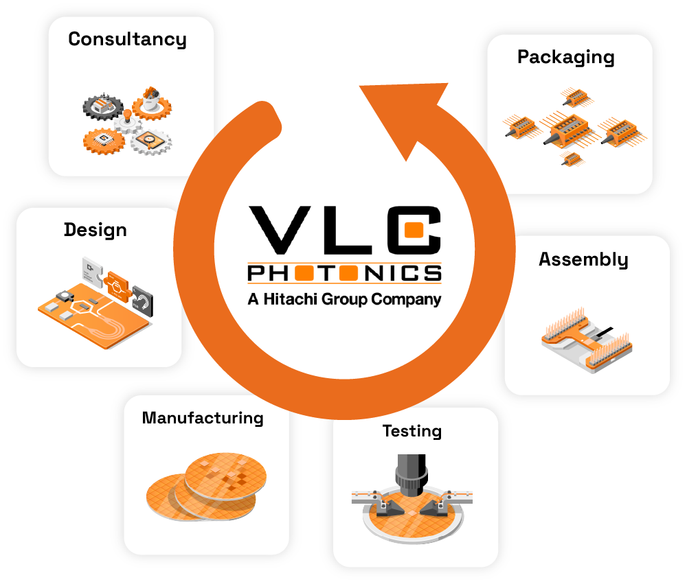
At VLC Photonics we empower the global PIC ecosystem with cutting-edge design and testing for Silicon Photonics and new material platforms.
Our expanded engineering services focus on yield, cost, reliability, and performance, helping you take PICs from concept to scalable production. Backed by Hitachi High-Tech’s global network, we align with your short-term needs and long-term vision.
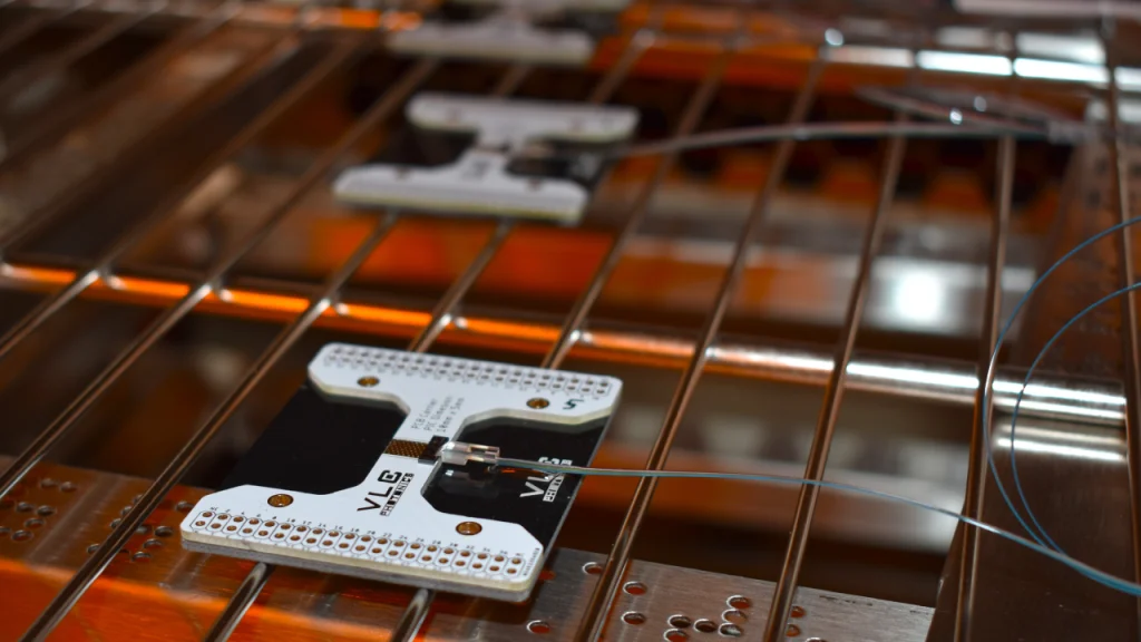
Photonics RF signal Characterization
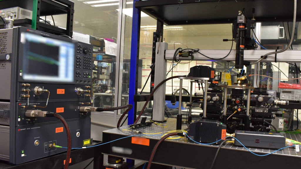
Ultra-High data rates for optical transceivers.
- True 112 GBaud PAM4 and NRZ for Eye Diagram & BER Testing. The only commercially available 2-ports 256 GSa/s AWG with >80 GHz analog bandwidth, ideal for generating up to 224 Gbps PAM4 signals and pushing toward 160 GBaud for R&D purposes. Real-Time Oscilloscope, 70 GHz, 10-bit instrument with 256 GSa/s sampling, enabling precise jitter, RIN-OMA and BER measurements. Supported by Keysight M8070ADVB Advanced Suite.
S-Parameters up to 110 GHz EO/OE Bandwidth
- Lightwave Component Analyzer for EO S-parameter measurements up to 110 GHz at 1310 & 1550 nm wavelengths. In-lab manual setup with calibration workflows validated to ensure consistency and setup reproducibility.
Delivering insights at the highest frequencies, ideal for next-gen photonic devices. Ready to push your PICs further? Contac us now!
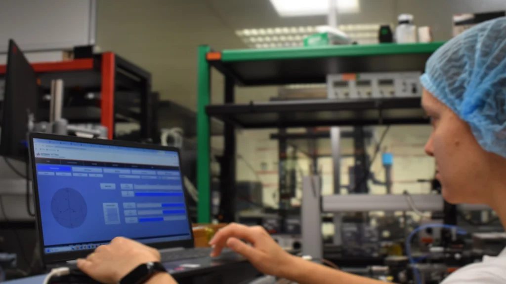
Photonic Automated Testing line
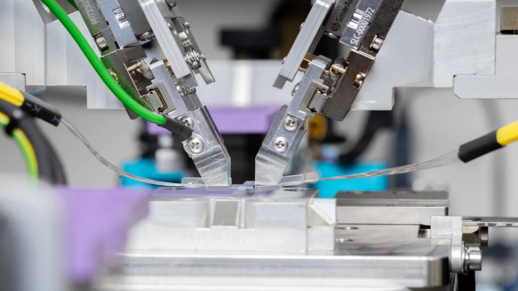
Opto-electro-RF data-acquisition at die or wafer level with automated recipe-based motion of optical probes with 6-axis active stage alignment and 40 nm linear motion resolution + electrical DC/RF probes 3-axis arms + dispenser for index matching gel or viscous solution (at die-level).
- Optical power stability: < 0.02 dB variation, and inter-die repeatability < 0.1 dB, at vertical gratings C-band polarization-maintaining.
- Sweeping faster than 10 seconds per measurement. 24/7 operation.
- Precise optical beam scanning and coupling maps (edge or vertical configurations).
- Temperature setting conditions up to 75 degrees Celsius.
Multi-DC probing, RF up to 67 GHz EO bandwidth.
x1 Die-Level | Tray-to-tray hands-off sorting
- Automated Pick & Place for binning of Known Good Dies (KGD) vs. underperformers.
- Dispenser for index-matching gel or viscous solutions. Enabling UV and epoxy-based optical coupling.
x2 Wafer-Level | Operator-loading
- Silicon 300 mm wafers down to below 2-inches Indium Phosphide bars or multi-chip trays of singulated bare dies or chip on carrier.
- Edge coupling via trench-embedded micro-periscope
- + 100 wafers capacity.
Automate and scale your photonic testing, without sacrificing accuracy Contact us now!
Advanced Instrumentation
Polarization Control
Stability and precision at every polarization state.
- Ensure long-term stabilized deterministic state of polarization, with real-time polarization tracking, across O-, C-, and L-bands (1240–1650 nm).
- Scrambling mode for random polarization fluctuations and quick dynamic tolerance tests in MZI-based modulators and polarization-dependent PIC circuits. Supporting PDL (loss) and PMD (mode dispersion).
Critical tools for polarization-sensitive systems in communications and sensing.
Optical Broad-Source
- UV-VIS-NIR Range: 400 – 2400 nm wavelength, with a spectral power of 0.6 mW/nm ( ) to 2.0 mW/nm ( ) over the visible band, and output total full-spectra power of 2.2 Watts.
- IR to MIR Range: 1300 – 4500 nm wavelength, with a spectral output total power +300mW, from which 110mW over the mid-IR band (2200 – 4200 nm).
Support for a broad range of applications, from biosensing to spectroscopy.
Die sorting from blue-tape wafer to gel-pak/carrier
- Automated Pick and Place System, supporting wafers up to 200 mm (potentially 300 mm). Compatible with waffle trays, gel-paks, and film frames. Die size range from 200 µm to 25 mm. Placement accuracy of ±120 µm and throughput up to 1.200 units/hour. Possibility to integrate visual inspection and QA traceability.
Reliability Testing
Identify early failures and evaluate long-duration device yield screening.
Thermal-humidity fatigue cycles
High Temperature Storage: MIL-883 1008.2, JESD22-A103, IEC 60749-6, ED-4701/201B
Low Temperature Storage: JESD22-A119, ED-4701/202
Thermal Cycling: MIL-883 101.8, MIL-STD/202G 107G, JESD22-A104, IEC 60749-25, ED-4701/100 105
Moisture: MIL-883 1004.7, ED-4701/203A, ED-4701/103, IEC 60068-2-30
Accelerated thermal life cycling (BDH, HTOL, HAST): From -80 ºC to +180 ºC (±0.2 ºC), and humidity rates of 5–95% (moisture at temperature range +10 ºC to +95 ºC). Continuous dynamic package monitoring by cable/pigtail connections or punctual pre/post stress static external characterization/comparison of bare dies or packages.
- Burn-in of bare dies or small packages in a rack with continuous dynamic electrical-biasing and optical-detection monitoring for lasers.
Visual & Failure Analysis
Techniques and instrumentation to catch defects with below 100 nm resolution.
- Design-to-manufacture validation, mechanical defect screening, early structural validation of fabrication issues, and root-cause tracing
- Cross-section and surface inspection with SEM, FIB, SDX (FEI-SEM: XL30 TMP, Hitachi SEM: TM4000Plus, and additional equipment via Hitachi High-Tech Europe).
From qualification to failure analysis, we help you ensure device robustness.
Custom III-V epitaxy Design
We design full epitaxial layer stacks, tailored to your device needs.
- From InP and GaAs heterostructures to advanced multi-quantum wells, our expertise in MOCVD and MBE ensures optimized performance for lasing efficiency, modulation bandwidth, and thermal stability.
Build your devices from the atom up, with full control over your materials.
Through TAVI platform, VLC Photonics offers a unique solution to develop III-V PICs. Learn more about TAVI here
FAQ
What is the maximum frequency range you support for RF characterization?
We support S-parameter and BER testing up to 110 GHz, with data rates up to 112 GBaud.
Can your automated die-level tester handle high volumes?
Yes, it is designed to test thousands of dies, with automated pick-and-place and fiber pigtailing.
What types of modulation formats can you test?
We support both PAM4 and NRZ modulation formats.
What materials do you work with for epitaxy design?
We specialize in III-V semiconductors, including InP, GaAs, and custom layer stacks.
How accurate is your power stability in automated testing?
Our system offers < 0.02 dB power variation and < 0.1 dB repeatability.
What environmental tests do you offer for reliability?
We provide thermal cycling, HTOL, shock, burn-in, HAST, and detailed failure analysis.
What wavelength ranges do your optical instruments cover?
We cover 400–2400 nm and 1300–4500 nm, including visible and MIR ranges.
Do you offer polarization control for dynamic systems?
Yes, including real-time stabilization, high-speed scrambling, and fast PDL measurement.
Ready to power up your photonic roadmap?
Whether you’re developing high-speed optical transceivers, advanced sensors, or complex PIC-based systems, VLC Photonics brings the tools, expertise, and automation to accelerate your innovation.