Testing photonic integrated circuits (PICs) poses unique challenges compared to traditional IC chip testing due to the requirement for both electrical and optical probing. This PIC testing can be conducted at the wafer level (Wafer Level Testing) or after the chip has been diced or cleaved (Die Level Testing). Precise alignment of optical probes with sub-micrometer precision is crucial for characterizing photonic waveguide components. VLC Photonics offers comprehensive manual and automated testing capabilities tailored to your project requirements.
Testing offerings:
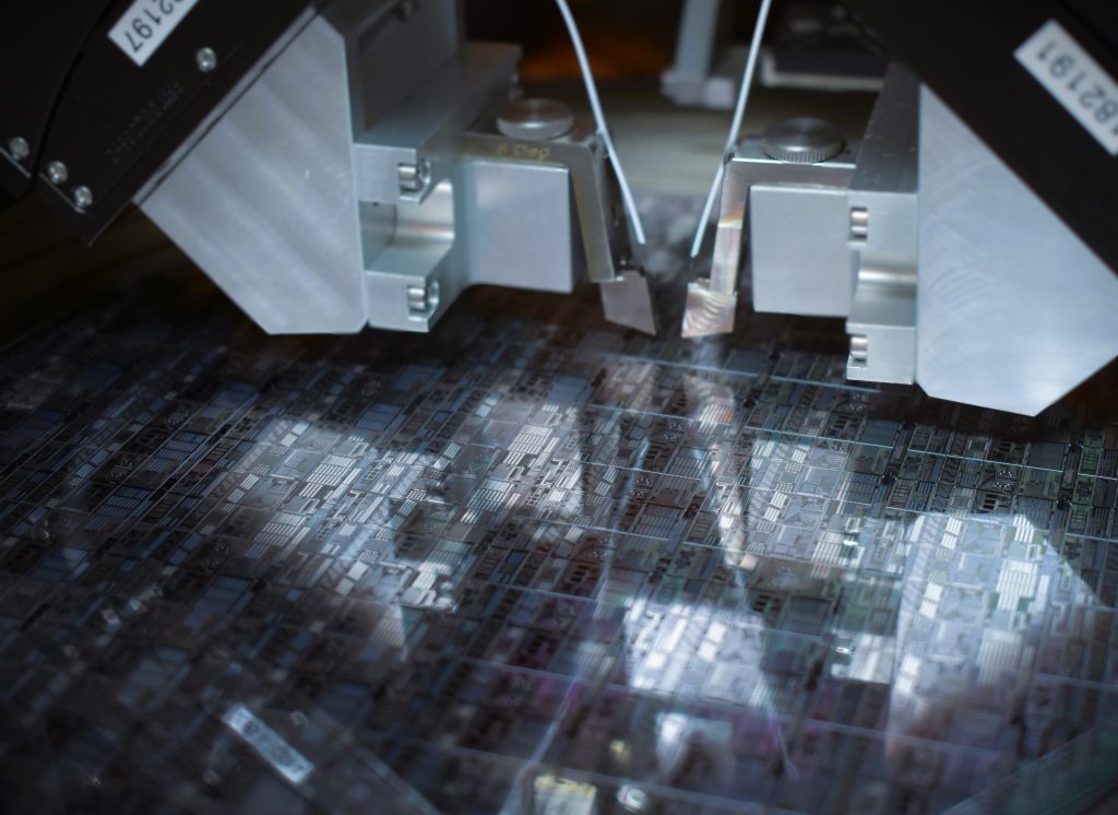
- Wafer Level Testing:
Involves the fully automated alignment of probes with nanometer precision, characterizing optical, electrical DC, and RF parameters. - Die Level Testing:
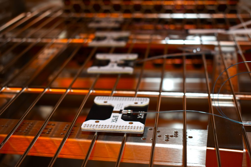
Testing for of diced or cleaved dies. Semi-automated setups allow for much greater flexibility in the characterization setup and the kind of experiments and measurements possible, while fully automated setups can accurately measure 100’s-1000’s of individual dies with great speed and repeatibility. - Packaged PIC Testing:
Chip-on-board (CoB) or Chip-on-carrier (CoC) assemblies allow for an easier measurement due to predefined connectorized inputs and outputs via electrical pins and optical fiber pigtails. Full characterization and testing services are also provided for packaged dies.
Services offerings:
Visual inspection:
Detailed visual inspection of packages, dies or bars, and wafers for any defects, including Scanning Electron Microscope (SEM) for in-depth analysis.
Design for Testing:
Expert advice on layout arrangement for optimal probing and measurement, best fiducials and alignment markers, and test structures, ensuring efficient testing processes.
Test Design Kits implemented as .pdf guidelines (request here), and as software implementations for the main photonic layout tools Luceda IPKISS and Synopsys Optocompiler
- Optimized Design for Testing → Ensures input and output ports (optical and electrical), fiducials and alignment markers, and test structures are properly positioned for seamless integration with standard automated testing procedures.
- Streamlined Testing Process → Encourages designers to consider testing from the start, reducing late-stage design modifications.
- Cost Reduction → Helps test houses minimize engineering expenses related to measurement setups.
- Faster Test Campaigns → Speeds up testing procedures, improving efficiency and lowering overall costs.
Optical probing:
Vertical coupling and edge-coupling are both possible at die and wafer level, using different types of optical probes for wavelengths, from visible to O/C/L bands and mid-IR.
Electrical probing:
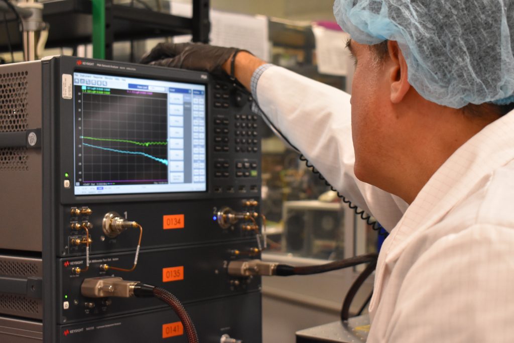
Electrical single and multi-contact probes for DC and RF up to 110 GHz.
In-Depth Analysis:
Comprehensive analysis of measurement traces, failure modes analysis, root cause analysis, and test reports for compliance with specifications.
Reliability testing:
Temperature cycling and burn-in, voltage and current stressing for accelerated lifetime testing.
High-Speed Signal: Eye Diagrams & BER Testing
Supporting PAM and NRZ modulation formats for data communication rates up to 112 Gbaud, with eye diagram analysis and Bit Error Rate (BER) measurements to validate signal quality and compliance.
Environmental testing:
If more extensive testing like e.g. environmental, radiation, mechanical (half sine, full wave vibration and shock tests) are required, we have partners who can support too.
Capabilities:
- Clean Room Laboratories:
Testing conducted in clean room laboratories by experienced engineers using state-of-the-art equipment. It is certified as ISO Class 6 (Class 1,000) with full ESD protection. - ISO 9001 Certification:
Adherence to ISO 9001 certified test processes, with proper calibration of instrumentation and redundancy in all equipment and components. - Optical Testing:
Complete optical testing with various light sources (lasers, supercontinuum, LEDs) spanning visible to near-infrared and mid-infrared wavelengths. - Electrical Testing:
DC and RF testing up to 110 GHz frequency, signal processing, and multi-probe testing stations. - Reliability Testing Services: Evaluate infant mortality with aging tests, including, temperature/current/voltage cycling, and burn-in testing. More advanced reliability tests for vibration, shock, radiation, etc. also available on demand.
- High-Speed Signal Generation and Real-Time Analysis: Waveform signal generation combined with a real-time oscilloscope featuring 100 GHz bandwidth and 256 GSa/s sampling rate on two independent channels, enabling precise evaluation of eye diagrams and Bit Error Rate for high-speed signal integrity assessment.