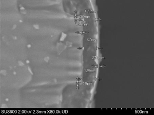
In photonic integrated circuits, fabrication precision at the submicron level is essential to ensure optimal optical performance. Even minor defects introduced during lithography, etching, deposition, or post-processing can significantly impact transmission efficiency and increase optical losses due to scattering. Among these, particulate contamination remains one of the most common and detrimental sources of performance degradation
Our SEM analysis services are conducted in ISO Class 6 (Class 1,000) certified facilities.
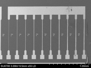
We utilize high-resolution scanning electron microscopy (SEM) to detect and document critical issues such as short circuits, surface cracks, delamination, edge roughness, and non-uniform layers. SEM offers a non-destructive, highly accurate method to assess multiple layers in a wafer, making it an ideal tool for both prototyping and production environments.
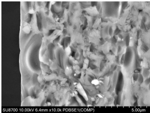
Beyond standard imaging, our team provides diagnostic SEM evaluations to assess the mechanical effects of dicing on chip cross-sections. We’ve observed how poor dicing can tear off layers or damage waveguides, and how transitioning to precision techniques like laser dicing or optimized saws can dramatically reduce these issues.
Whether you’re validating a wafer-level process, designing or characterizing a photonic device or components, we support you with:
High-resolution SEM imaging
Contamination diagnosis and cleaning guidance
Dicing damage assessment
Ion milling to enhance surface morphology
Metal layer defect identification
Full-wafer inspection using CD-SEM
Expert reporting and consulting tailored to PIC technologies
Fast turnaround with personalized support
SEM-driven feedback to inform PIC design and manufacturing decisions
Explore the specifications here
Talk to our expert!
We comply with industry standard design techniques for manufacturability, testability and packaging. Moreover, your intellectual property will always be confidential and secured, and any IP developed through the integration process can be transferred to you on demand.