TAVI (Taper-Assisted Vertical Integration) is a regrowth-free, monolithic InP integration platform that enables customers to combine active and passive photonic functions on a single chip.
Active + Passive Photonics. One Platform. At Scale
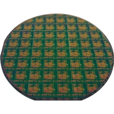
Monolithic photonic integration in InP
Active and passive waveguide devices are co-processed over the same substrate.
Vertical Integration
Functionally different waveguide devices are defined at different vertical guiding levels, which are integrated into a common epitaxial structure.
Evanescent-field coupling
Evanescent-field coupling is used between the waveguides to form a vertically integrated photonic circuit.
Regrowth-free process
Active and passive waveguide devices are co-processed over the same substrate.
Epitaxy and fabrication are decoupled and can be delivered independently
Decoupling of the epitaxial growth and wafer fabrication allows for outsourcing each of them to high-volume, industrial grade foundries (epitaxy or wafer fabs), providing a high-yield path to production.
Applications
Datacom and Telecom transceivers and Co-packaged Optics
Hybrid Photonic Integration
RF Photonics and Quantum
Why TAVI makes a difference
TAVI delivers high yield, scalability, and a clear path to production, while reducing adoption risks through its unique business model.
From proof of concept ➝ engineering ➝ high-volume manufacturing, customers can scale seamlessly without the barriers of traditional approaches.
TAVI offering for custom PICs
-
World’s #1 independent epitaxy supplier: known good wafers, low-risk and on-time epitaxy procurement.
-
Designs compatible with the commercially available and yet decoupled epitaxial growth and regrowth-free wafer fabrication processes.
-
Industrial grade wafer fabrication foundry: mature process, clear design rules, 24/7 operations controllable yields.
-
PDK with component library, enabling for migration from the device physics and fabrication process to the circuit design and process integration.
-
Comprehensive library of pre-verified and standardized functional waveguides and devices/components formed with them, a.k.a. building blocks.

