EO characterization of PIC has become a critical bottleneck in the development of 800G and 1.6T optical transceivers. The modulator and photodetector components inside these systems need to demonstrate electro-optical bandwidths of 70 GHz or more, and measuring them correctly requires instrumentation that actually reaches those frequencies. This article describes the calibrated VNA + LCA methodology used at VLC Photonics for EO and OE S-parameter measurement up to 110 GHz, with experimental results on a TFLN modulator and a commercial high-speed photodetector.
This post walks through the measurement methodology and results for two device types: a thin-film lithium niobate (TFLN) Mach-Zehnder modulator with EO bandwidth exceeding 110 GHz, and a high-speed photodetector from Albis Optoelectronics characterized across a range of bias conditions. Both were measured using a Keysight VNA + LCA solution at VLC Photonics, covering 10 MHz to 110 GHz.
| A test setup that tops out at 40 or 67 GHz does not characterize an 800G device; it characterizes the ceiling of your instruments. |
EO characterization vs OE characterization: what’s the difference?
Before getting into the setups, it’s worth being clear about what these two measurements are and why they require different configurations.
Electro-optical (EO) characterization measures how efficiently an electrical RF signal is converted into optical modulation. The primary figure of merit is the S21 magnitude versus frequency, the EO bandwidth. This applies to transmitters: MZM, EAM, directly modulated lasers, TOSA.
Opto-electrical (OE) characterization measures the reverse: how efficiently the device converts incoming optical modulation back into an electrical signal. Again, S21 is the key parameter, but now it represents the responsivity roll-off with frequency. This applies to receivers: PIN photodiodes, APDs, ROSA, PIN-TIA integrated receivers.
Both measurements extract scattering parameters, but the role of the optical and electrical ports is reversed. The instrument configuration and the calibration must reflect that.
Electro-optical characterization of a TFLN modulator
Why TFLN?
Silicon photonics modulators based on plasma dispersion are bandwidth-limited by carrier dynamics. Thin-film lithium niobate (TFLN) avoids this constraint through its strong Pockels effect, enabling linear, low-chirp modulation well beyond the limits of plasma-dispersion-based silicon photonics. Recent demonstrations have shown EO bandwidths exceeding 100 GHz, positioning TFLN as a primary candidate for next-generation 800G and 1.6T transceivers, coherent systems, and co-packaged optics (CPO) modules.
Measurement setup
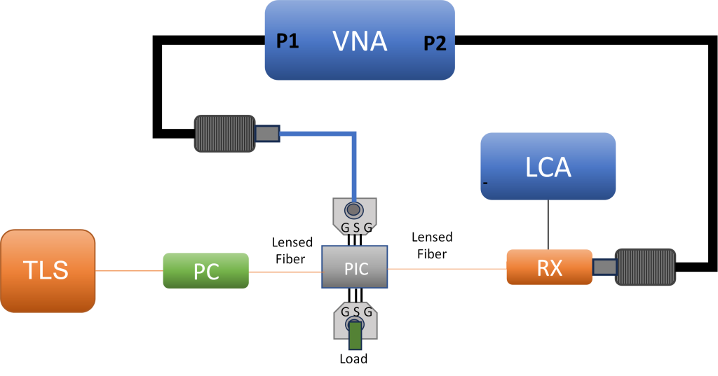
The EO setup uses a tunable laser source (TLS) at 1550 nm, combined with a polarisation controller (PC) to ensure TE-polarised input to the modulator. The RF stimulus from Port 1 (P1) of the Vector Network Analyser (Keysight N5227B) is applied to the PIC via a Ground-Signal-Ground (GSG) RF probe. The resulting modulated optical signal is recovered by the LCA receiver (Keysight N4372E) and fed back to Port 2 (P2) of the VNA. Optical coupling in and out of the PIC uses lensed fibres. A 50 Ω termination load on a second GSG probe is essential: without it, reflections at the modulator output degrade the apparent bandwidth.
Results
The S21 magnitude of the TFLN modulator remains within the 3-dB band across the entire 0–110 GHz sweep. The bandwidth of the device exceeds the measurement capability of the setup; we are limited by the instrument, not the modulator. The S11 parameter stays below −10 dB across the full frequency range, confirming good impedance matching with the added termination.
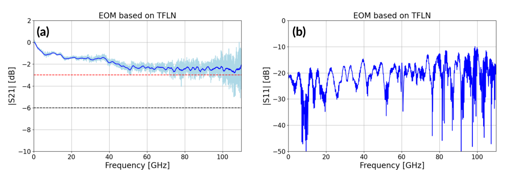
The TFLN modulator used in this characterization was provided by Luxtelligence
| The TFLN modulator’s EO 3-dB bandwidth exceeds 110 GHz, beyond the upper frequency limit of the present setup. Fully resolving the bandwidth of state-of-the-art TFLN and InP modulators requires instrumentation above 110 GHz. |
Opto-electrical characterization of a high-speed photodetector
Device under test
High-speed integrated photodetectors from Albis Optoelectronics were selected to demonstrate OE characterization across the full 110 GHz range. These devices are representative of the high-speed receiver components used in advanced transceiver modules and co-packaged optics (CPO) assemblies.
Measurement setup
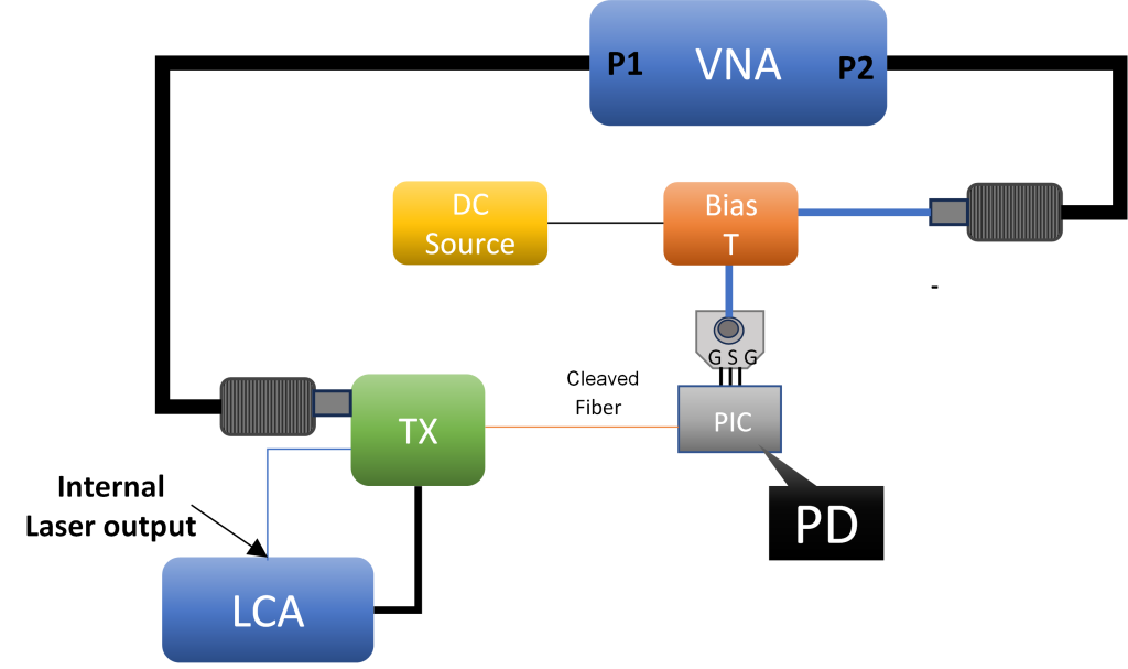
In the OE configuration, the LCA’s internal continuous-wave laser serves as the optical source. A calibrated reference transmitter (TX) intensity-modulates the optical signal using the RF stimulus from VNA Port 1. The modulated signal is coupled into the photodetector (PD) via a cleaved fiber matched to the input geometry of the device. The photocurrent at the PD output is recovered through a GSG RF probe and routed to VNA Port 2.
A bias-tee is inserted in the RF path: this passive component, formed by an inductor and a capacitor, combines a DC voltage from an external source with the RF photocurrent, allowing simultaneous biasing and broadband signal extraction. High-speed photodetectors must operate under reverse bias to maximize bandwidth and responsivity, so the bias-tee is not optional — it’s essential for an accurate measurement.
Results: The impact of bias voltage
The results make clear why operating conditions are not optional metadata in photodetector characterization. At 0 V bias, the 3-dB OE bandwidth is approximately 18 GHz. At −2 V reverse bias, the same device reaches 75 GHz — a 4× improvement driven by the reduction of depletion-region transit time and junction capacitance at higher reverse voltage.
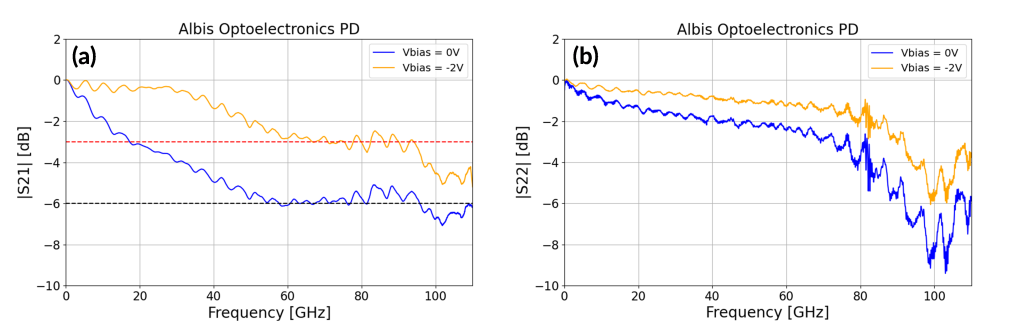

A quasi-flat response is observed between 60 and 90 GHz at the 3-dB level. The S22 parameter improves with bias, confirming better output impedance matching and maximum recovery of the electrical signal at the PD output.
| Reporting photodetector bandwidth without specifying the bias operating point is incomplete and potentially misleading. The same device delivered 18 GHz at 0 V and 75 GHz at −2 V. |
What this means for your testing strategy
- Your instrument bandwidth must exceed your device bandwidth. If your test setup tops out at 40 or 67 GHz, you cannot characterize components designed for 800G. The measurement ceiling of your instruments becomes the reported bandwidth of your device. Fully characterizing TFLN modulators and high-speed InP photodetectors requires instrumentation that reaches above 100 GHz.
- EO and OE are separate measurement workflows. They use different optical configurations, different VNA port roles, and different calibration procedures. A single generic setup cannot cover both correctly. Make sure your test partner has both configured and calibrated independently.
- Bias conditions determine what you measure. For photodetectors, the 3-dB bandwidth is a function of the operating point. Test at the target reverse bias, not at 0 V.
- S11 and S22 matter as much as S21. Impedance matching at the RF input and output directly affects system-level performance. Both parameters should be extracted and reported alongside bandwidth figures.
| Explore our testing capabilities |
Acknowledgements
VLC Photonics acknowledges Albis Optoelectronics AG for providing the high-speed photodetectors evaluated in this work, and the support of the INSPIRE project (“Fotónica Integrada Transversal como Transformador Deep Tech de Industrias Estratégicas”), funded by CDTI within the “Programa de Misiones de Ciencia e Innovación” linked to the PERTE for Microelectronics and Semiconductors, 2023 call.


