In this article, you will find real-case scenarios where significant limitations were encountered during SEM analysis of photonic chips. Issues such as carbon contamination, mechanical damage from dicing, errors during Focused Ion Beam (FIB) milling, mask misalignment, and excessive surface roughness are discussed.
Let´s identify the most common pitfalls in SEM-based inspection of photonic samples, illustrate them with practical examples, and extract useful recommendations to improve the reproducibility and reliability of the analysis.
How does carbon contamination affect SEM analysis in photonics?
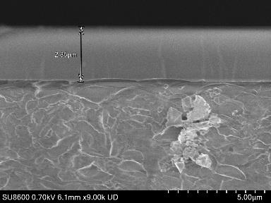
During SEM inspection, severe carbon contamination was observed (Fig. 1), which prevented the acquisition of clear images. The SEM operator confirmed the presence of carbon-based residues on the sample surface, likely originating from organic contaminants left on the chip.
What tools can remove hydrocarbon residues before SEM inspection?
To tackle this, the sample was cleaned using the ZONESEMII Tabletop Sample Cleaner, which employs vacuum-controlled UV irradiation and activated oxygen to eliminate hydrocarbon contamination. However, the cleaning proved insufficient, suggesting either an especially resistant residue or inadequate treatment. Under the electron beam, carbon buildup obscured fine structural details, rendering the images unusable.
This highlights the importance of thorough cleaning prior to SEM analysis, as poor sample preparation can severely compromise image quality and data reliability.
Why is sample preparation essential before SEM inspection of photonic chips?
When working at the nanoscale, a single layer of unwanted material can ruin the party. That’s exactly what happens when carbon contamination sneaks in during SEM analysis of photonic integrated circuits (PICs).
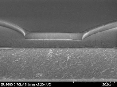
In Fig. 2, the same structure is shown, but the sample was taken just before deposition of the top layer. In this case, the image exhibits higher resolution, allowing clearer visualization of structural features.
Key takeaway for PIC engineers: If you’re using Scanning Electron Microscopy for photonic devices, meticulous sample cleaning is the unsung hero. Don’t let invisible dirt sabotage your nanostructures.
Impact of dicing quality SEM imaging of Photonic Chips
If you are asking if poor dicing can compromise SEM cross-sectional analysis of photonic devices, the answer is a big yes!
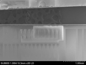
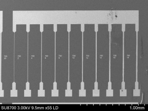
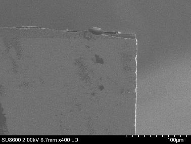
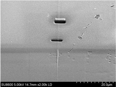
One of the biggest issues we found during SEM analysis was the poor dicing quality of the chips. The cross-sectional images show very rough and damaged edges (Fig. 3), and in many areas, critical layers like the top oxide are missing completely or partially.
This kind of surface damage makes it hard to identify the layer stack and see key structures like the waveguides. Even with optimized SEM settings, low voltage, and good contrast, the surface was too fractured to get reliable images. In some cases (Fig. 4 and Fig. 5), entire layers were torn off during the cut. In others (Fig. 6), the waveguide was still visible, thanks to a cleaner cut.
There was also some hydrocarbon contamination, but the main problem was the mechanical damage from dicing. While cleaning can help with contamination, it can’t fix structural damage.
This shows the need to use better dicing methods, like laser cutting or well-tuned saws, to avoid damaging the sample and to get usable SEM results.
Issues in FIB-SEM Characterization of Waveguides
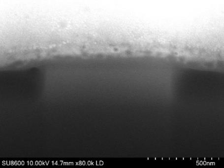
Different FIB cut conditions were tested. The best results were obtained with a narrow cut and platinum deposition, which minimized damage and provided clean imaging (Fig. 7).
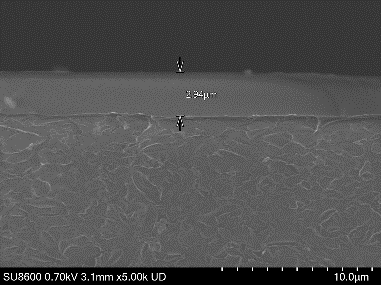
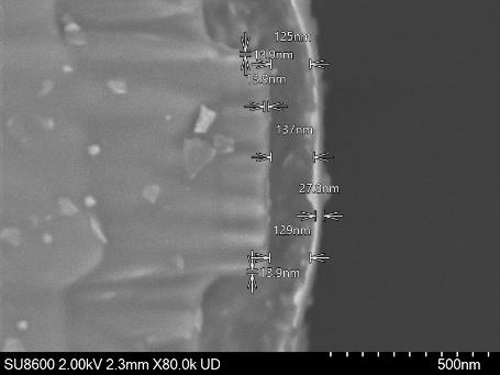
An attempt to identify the layer stack from the FIB cross-section was made (Fig. 8), but the contrast was insufficient to clearly resolve all layers. Imaging from the cleaved chip edge provided better visibility (Fig. 9). A ≈14 nm oxide layer was observed around the SiN waveguide. The SiO₂ layer measured 137 nm instead of the expected 100 nm, and the aluminum, expected as two 40 nm layers, appeared as a single ≈30 nm layer. These deviations were reported for process improvement.
Can Ion Milling improve surface morphology for SEM Imaging?
Absolutely, and we’ve tested it. Using the airBlade 5000 with a high-speed Ar ion gun, capable of milling silicon at 1 mm/hour with a width of up to 8 mm, we’ve successfully improved surface conditions on photonic samples.
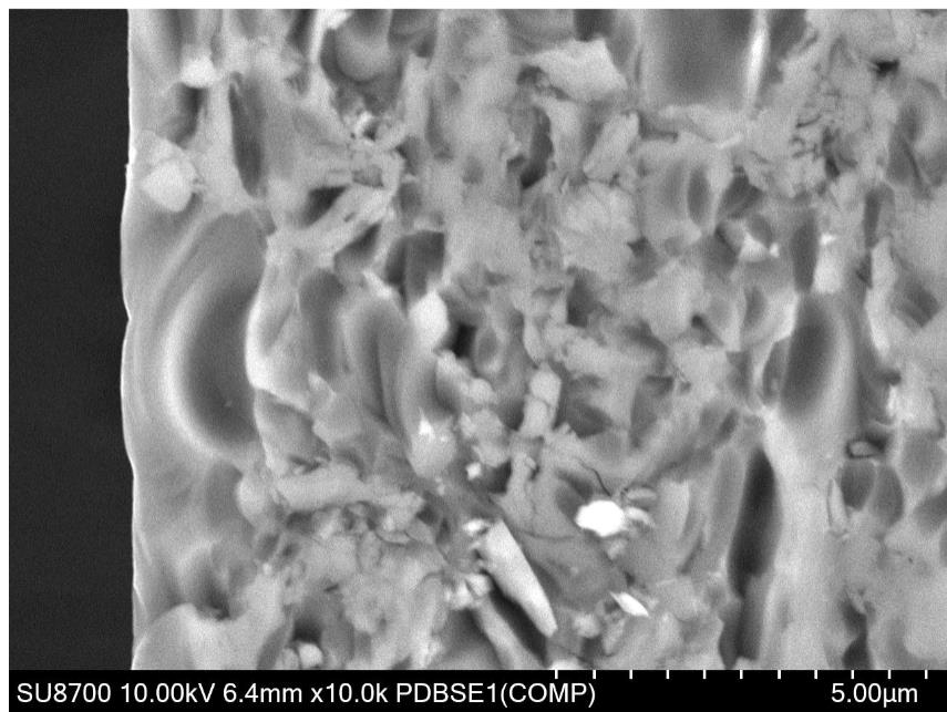
Before treatment (Fig. 11), SEM images showed severe surface roughness, with collapsed structures and debris forming a mesh-like pattern. This severely hindered imaging clarity and feature detection.
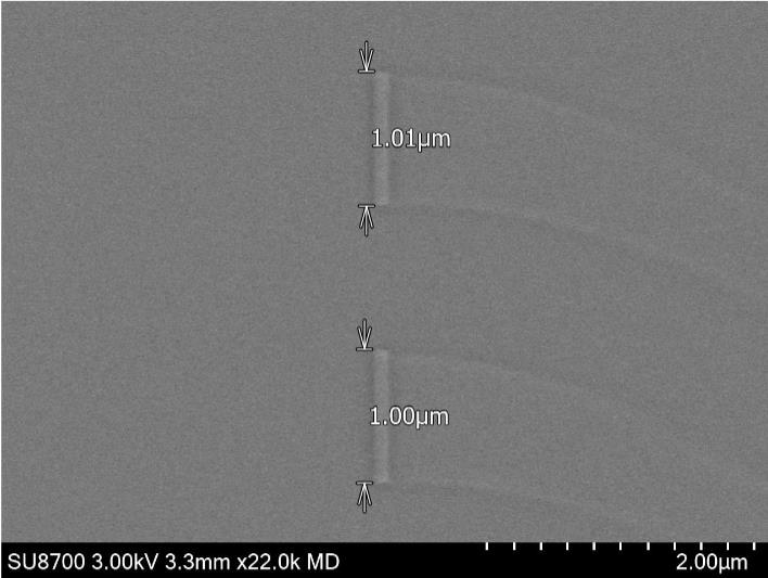
After Ion Milling, the same surface appeared flat and clean (Fig. 12), allowing us to clearly resolve and measure etched structures as small as 123 nm and up to 1.00 µm. This highlights Ion Milling as a powerful technique for SEM sample preparation, particularly when accurate dimensional analysis is needed.
Avoid contamination. Prevent damage. Get clear results.
At VLC Photonics, we know that when it comes to Scanning Electron Microscopy (SEM) for photonic integrated circuits (PICs), there’s no room for guesswork. Blurry images, missing layers, or structural artifacts can compromise everything, from your process monitoring to your final device qualification.
That’s why we offer state-of-the-art SEM analysis services designed specifically for PICs, with a strong focus on sample integrity and imaging quality.