This article presents a non-destructive methodology for analyzing the physical properties of photonic waveguides using Scanning Electron Microscopy (SEM). SEM is a powerful tool that enables detailed dimensional measurements and defect detection across different wafer locations. The focus is on evaluating key parameters such as line edge roughness, surface irregularities, and sidewall features, which can influence both optical performance and manufacturing consistency. By supporting simulations and production processes, SEM analysis contributes to maintaining and improving the quality of waveguide design and fabrication. Several examples are provided to illustrate the types of variations observed in fabricated structures and their relevance for design feedback and process optimization.
In photonic integrated circuits (PICs), waveguide geometry plays a crucial role in determining optical performance. However, differences in waveguide geometry can often be observed across a single wafer due to several fabrication-related factors. These variations are not just cosmetic, they can significantly impact the optical propagation losses, mode confinement, and device yield.
One of the most effective techniques to analyze such dimensional differences is Scanning Electron Microscopy (SEM). This high-resolution imaging method allows for detailed observation of line edge variation, surface roughness, and sidewall defects, which are key parameters affecting light propagation in waveguides.
Why does waveguide geometry vary across a wafer?
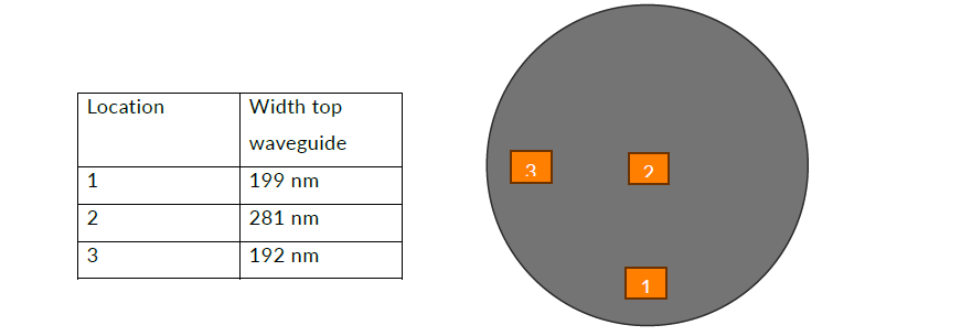
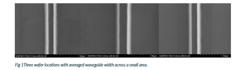
Various reasons can contribute to waveguide variation across wafers or even between different locations within the same wafer. Below is the summary of one wafer’s waveguide width measurements:
What is line edge error (LER) in waveguides?
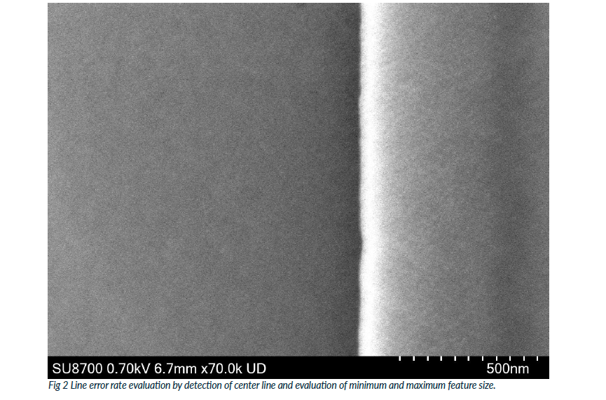
Line Edge Error (LER) refers to the small-scale variations in the edge of a waveguide from its intended design. These fluctuations may appear minor under the microscope, but they can significantly impact the optical performance of the waveguide by introducing scattering losses and mode distortion.
In this case, a variation of 84 nm is observed, or ±42 nm from the center line (expected design).
How does a ±42 nm deviation in waveguide edges influence device behavior?
This degree of LER can cause:
- Increased propagation losses due to sidewall scattering.
- Mode mismatch in tightly confined structures.
- Phase errors in interferometric circuits.
Minimizing LER is crucial during fabrication to ensure that light confinement and propagation remain within design tolerances, especially in high-density photonic integrated circuits.
How does waveguide top surface roughness impact performance?
Various features and defects on the top, bottom, and side surfaces of waveguides affect performance. SEM allows evaluation of feature size on the top surface, which can later be used in simulation models to estimate waveguide performance.
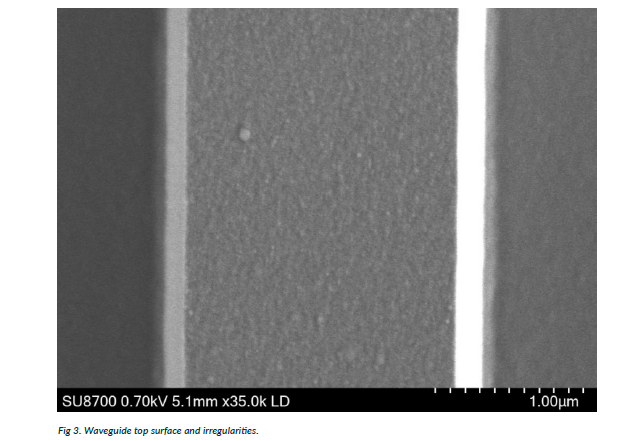
Larger feature size marked by number 1 is 154 nm, where small irregularities are from 10 to 30 nm.
Why is SEM analysis crucial for surface roughness evaluation?
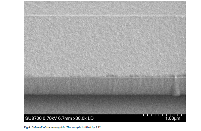
Sidewall roughness evaluation is more complex, as the sample must be tilted to assess the dimension of features. Post-processing is needed to calculate actual sizes based on trigonometry using the detector angle. In the image below feature size can be evaluate to be 12-25 nm size on side wall, and larger defect can be seen in the right corner of the image being over 200 nm in width at larges point.
Large particles and defects
The interpretation of how these features affect performance is complex, but tracking and collecting statistics about them is valuable. Simulations evaluating these features are also complex, since they must consider not only one particle but also their quantity and spatial distribution, which can create resonant effects.
Conclutions
Variations in line error and surface roughness can be evaluated using Scanning Electron Microscopy and fed into various models to improve productivity and device fabrication processes.
Several types of stakeholders benefit from SEM image analysis:
- Optical designers: to consider roughness in simulations
- Fabrication teams: to adjust processes and match GDS-designed widths through
high-volume image capture (especially using CD-SEM) - Manufacturers: to track tolerances by measuring particle counts and controlling
large features if quantity or size exceeds acceptable thresholds
Surface roughness on top or sidewalls also impacts waveguide guiding properties,
especially depending on whether light propagates in TE or TM polarization.
What to know more? Read about the challenges in SEM Analysis of photonics chips here