Introduction
Using integrated photonics chips instead of discrete components offers significant advantages in terms of cost, chip footprint, and scalability, three critical factors that determine product-market fit and the success of any photonic product development.
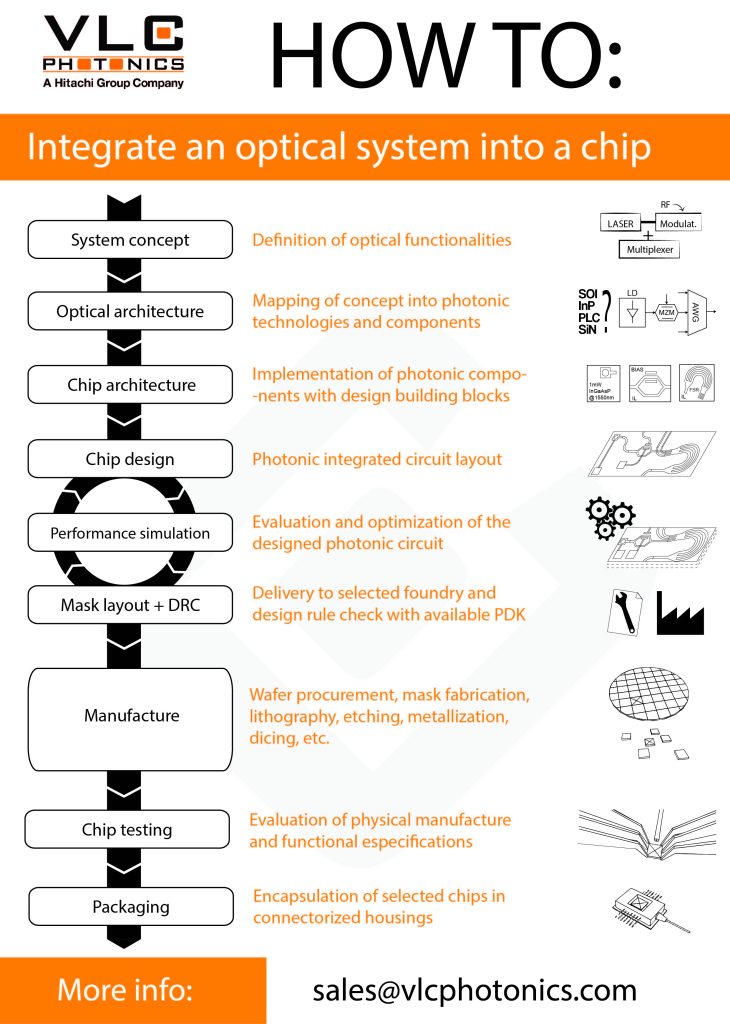
This step-by-step diagram illustrates the full process of integrating an optical system into a photonic integrated circuit (PIC), from initial concept to final testing and packaging. Each phase is critical to ensure functionality, manufacturability, and performance.
Conclusion
Designing and fabricating a photonic integrated circuit (PIC) is a highly specialized process that requires expertise across multiple domains—from architecture to testing and packaging. Every step must be carefully managed to reduce development risks, control costs, and accelerate time-to-market.
At VLC Photonics, we provide end-to-end engineering services tailored to your needs, across all material platforms and application areas. Whether you’re just starting or optimizing an existing design, our experienced team is here to support your success.
Contact us at sales@vlcphotonics.com to bring expert support to your PIC development journey.